- 您现在的位置:买卖IC网 > Sheet目录362800 > EVAL-AD1990EB (Analog Devices, Inc.) Audio Switching Amplifier
AD1990
POWER STAGE
The H-Bridge
The output stage of the AD1990 includes four integrated
MOSFET devices arranged in a full H-bridge, as shown in
Figure 23. The P-Type, high-side transistor of one leg and the
N-Type, low-side transistor of the opposite leg switch on and off
as a pair producing a total voltage swing across the load of
PV
DD
to +PV
DD
. The drive is floating and differential, and it is
important that neither output terminal be shorted to ground.
Rev. 0 | Page 13 of 16
The power supply for the output stage of the AD1990, PV
DD
,
should be in the 8 V to 20 V range and should be capable of
supplying enough current to drive the load. Connect the power
supply across the PVDD and PGND pins. The feedback pins,
NFR+, NFR, NFL+, and NFL, supply negative feedback to the
modulator as described in the Setting the Modulator Gain section.
For reactive loads, the impedance can only be below the
recommended threshold over a small portion of the amplifier’s
bandwidth. In these cases, the amplifier can enter overcurrent
shutdown in response to even small input signals in those
frequency bands. When designing a system, use the minimum
load impedance over the entire range of amplified frequencies
when calculating current output rather than the average or
nominal load impedance ratings often cited by loudspeaker
driver manufacturers.
Output Transistor Nonoverlap Time
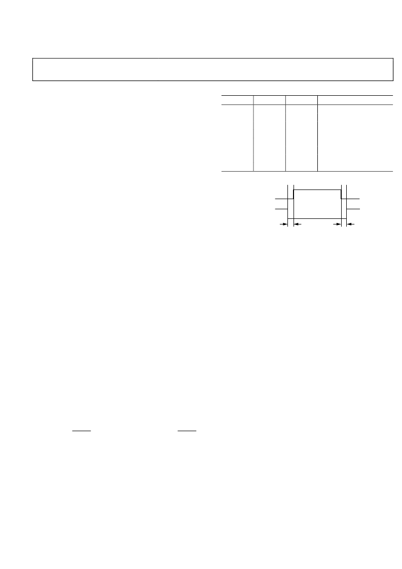
The AD1990 allows the user to select from one of eight different
nonoverlap times, as shown in Figure 24. Nonoverlap time
prevents or minimizes the period during which both the high-
side and low-side devices are on simultaneously due to propagation
delays and nonzero rise and fall times. If both the upper and
lower portions of a half-bridge conduct simultaneously, there is a
path directly from the power supply to ground and an induced
current flow known as shoot-through. However, introducing
this delay increases distortion by pushing the switching pattern
further from an ideal two-state waveform. Selecting the
nonoverlap delay requires a compromise between distortion
and efficiency. The logic levels on the three delay control pins,
DCTRL2, DCTRL1, and DCTRL0, set the nonoverlap time
according to Table 12. The state of DCTRL[2:0] is read on the
rising edge of RESET and should not be changed while RESET
is logic high.
Table 12. Nonoverlap Time Settings
DCTRL2
DCTRL1
0
0
0
0
0
1
0
1
1
0
1
0
1
1
1
1
DCTRL0
0
1
0
1
0
1
0
1
Nonoverlap Time (ns)
1
62
49
37
24
15
13.5
12
9
1
Values are typical and are not production tested.
HIGH-SIDE
GATE DRIVE
LOW-SIDE
GATE DRIVE
t
NOL
t
NOL
0
Figure 24. Half-Bridge Nonoverlap Delay Timing
The shortest setting (DCTRL[2:0] = 111) or the second shortest
setting (DCTRL[2:0] = 111) is recommended for most applications.
These two settings allow a small trade-off between efficiency
and distortion. Longer nonoverlap times generally increase
distortion while providing little or no decrease in shoot-
through current.
CLOCKING
The AD1990 Σ-Δ modulator requires an external clock source
with a nominal frequency of 12.288 MHz. This clock can come
from a crystal or from an existing clock signal in the application
circuit. The discrete time portions of the modulator run internally
at 6.144 MHz, corresponding to 128 × f
S
, where f
S
= 48 kHz.
As mentioned in the Σ-Δ Modulator section, the modulator has
a noise-shaping effect such that SNR is increased within the
audio band by shifting modulator quantization noise upward in
frequency. For an external clock frequency of 12.288 MHz, the
modulator’s noise-shaping works in a manner that results in a
flat noise floor at the amplifier output for frequencies 20 kHz
and below. Above 20 kHz, the amplifier noise rises due to the
spectral shaping of the modulator quantization noise. At very
high frequencies, the noise floor levels off and decreases due to
poles in the modulator noise-transfer function and in the
external LC filter.
The clock frequency does not have to be exactly equal to
12.288 kHz and can vary by up to ±10%. For other rates, the
noise corner scales linearly with frequency. When the modulator
runs at a rate lower than nominal, the average power stage
switching frequency decreases, the efficiency increases slightly,
and the noise floor begins to rise at a slightly lower frequency.
Likewise, a faster clock gives slightly increased bandwidth and
slightly lower efficiency.
发布紧急采购,3分钟左右您将得到回复。
相关PDF资料
EVAL-AD1992EB
Audio Switching Amplifier
EVAL-AD1994EB
Audio Switching Amplifier
EVAL-AD421EB
Loop-Powered 4 mA to 20 mA DAC
Eval-AD5025EBZ
Fully Accurate 12-/14-/16-Bit VOUT DAC SPI Interface 2.7 V to 5.5 V in a TSSOP
Eval-AD5045EBZ
Fully Accurate 12-/14-/16-Bit VOUT DAC SPI Interface 2.7 V to 5.5 V in a TSSOP
Eval-AD5065EBZ
Fully Accurate 12-/14-/16-Bit VOUT DAC SPI Interface 2.7 V to 5.5 V in a TSSOP
EVAL-AD5066EBZ
Fully Accurate 16-Bit UnBuffered VOUT DAC SPI Interface 2.7 V to 5.5 V in a TSSOP
EVAL-AD5379EB
40-Channel, 14-Bit, Parallel and Serial Input, Bipolar Voltage-Output DAC
相关代理商/技术参数
EVAL-AD1992EB
制造商:AD 制造商全称:Analog Devices 功能描述:Audio Switching Amplifier
EVAL-AD1994EB
制造商:Analog Devices 功能描述:EVAL BOARD FOR AD1994 - Bulk
EVAL-AD1994EBZ
制造商:Analog Devices 功能描述:EVAL BD CLASS D AUDIO POWER OUTPUT STAGE - Bulk
EVAL-AD22305
制造商:Analog Devices 功能描述:AD22305EVAL - Bulk
EVAL-AD22305X
制造商:Analog Devices 功能描述:AD22305EVAL (X GRADE) - Bulk
EVAL-AD2S1200CB
制造商:Analog Devices 功能描述:EVALUATION BOARD I.C. - Bulk
EVAL-AD2S1200CBZ
功能描述:BOARD EVAL FOR AD2S1200 RoHS:是 类别:编程器,开发系统 >> 评估演示板和套件 系列:- 标准包装:1 系列:PSoC® 主要目的:电源管理,热管理 嵌入式:- 已用 IC / 零件:- 主要属性:- 次要属性:- 已供物品:板,CD,电源
EVAL-AD2S1200SDZ
功能描述:BOARD EVAL FOR AD2S1200 RoHS:是 类别:编程器,开发系统 >> 评估演示板和套件 系列:- 标准包装:1 系列:- 主要目的:电信,线路接口单元(LIU) 嵌入式:- 已用 IC / 零件:IDT82V2081 主要属性:T1/J1/E1 LIU 次要属性:- 已供物品:板,电源,线缆,CD 其它名称:82EBV2081